
| Process | Process | Internal capacity | Routine regulation | Graphical representation |
| Cutting and splicing | Cutting and finished plate thickness | Layer number | 2~6 Layer(Laminated board) |
|
| 2~10 Layer(Hard and soft joint plate) | ||||
| 1~8 Layer(Soft plate) | ||||
| Opening panel size |
250*(220~400)mm 500*(220~400)mm |
|||
| Finished plate size (maximum) | 480mm*380mm | |||
| Finished plate size (minimum) | 5mm*8mm | |||
| Maximum sheet thickness (copper on both sides) | 0.3mm | |||
| Minimum sheet thickness (copper on one side) | 0.05mm(Finished product) | |||
| Other auxiliary materials | Pressure sensitive adhesive material specification |
Pressure-sensitive adhesive: 30/50/100/130um |
|
|
| Specification of thermosetting adhesive material | Thermosetting adhesive: 12.5/15/25/40/50um | |||
| PI reinforcement (excluding glue) material specification | PI:1.0 - 13mil | |||
| Specification of pet reinforcement (excluding glue) material | White:0.05-0.25mm | |||
| Transparent:0.025-0.25mm | ||||
| FR-4 reinforcement (excluding glue) material specification | FR-4:≥50um | |||
| Type of other reinforcement materials | Stainless steel, aluminum plate, nickel steel sheet according to customer requirements | |||
| Common plates | Material type |
Single and double-sided adhesive Single and double-sided adhesive free and halogen-free Single and double-sided adhesive without halogen |
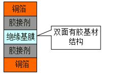
|
|
| Base copper thickness (electrolytic or calendered) | 1/3oz 1/2oz 1oz 2oz | |||
| Substrate PI | 0.5mil,0.7mil,0.8mil, 1mil,2mil |
| Working procedure | Item | Internal capacity | Routine regulation | Graphical representation | ||||||||||||||||||||||||||||||||
| Working edge size | Double sided tin deposition, gold deposition, OSP, tinplate | TD direction 10 / 6mm, MD direction 6mm (plywood fixed at TD side, 10 mm) |
|
|||||||||||||||||||||||||||||||||
| Single and double-sided electro gold plate (250mm direction) | 7mm | |||||||||||||||||||||||||||||||||||
| Single side tin, gold, OSP board | Long side / short side ≥ 6mm | |||||||||||||||||||||||||||||||||||
| TFT products with fine fingers facing outward | Long side / short side ≥ 7mm, and TD side clamp ≥ 10 mm | |||||||||||||||||||||||||||||||||||
| Multilayer hard and soft combination board | Long side / short side ≥ 12mm | |||||||||||||||||||||||||||||||||||
| Drill hole | Drilling tolerance | Location tolerance | Primary drilling: ± 0.05mm |
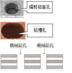
|
||||||||||||||||||||||||||||||||
| Secondary drilling: ± 0.1mm | ||||||||||||||||||||||||||||||||||||
| Laser drilling (minimum blind hole) | Ø0.08mm | |||||||||||||||||||||||||||||||||||
| Laser drilling (minimum through hole) | Ø0.05mm | |||||||||||||||||||||||||||||||||||
| Mechanical drilling hole diameter (minimum) | Ø0.1mm | |||||||||||||||||||||||||||||||||||
| Mechanical drilling hole diameter (maximum bit) | Ø6.30mm | |||||||||||||||||||||||||||||||||||
| Slotted hole (minimum) | Ø0.60mm | |||||||||||||||||||||||||||||||||||
| Finished hole diameter tolerance (plated through hole) | ±2mil(±0.05mm) | |||||||||||||||||||||||||||||||||||
| Finished hole diameter tolerance (non plated through hole) | ±1mil(±0.025mm) | |||||||||||||||||||||||||||||||||||
| Hole metallization | Black hole, PTH / plating | PTH hole minimum hole wall average copper thickness | Double sided board:10--18um |
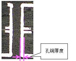
|
||||||||||||||||||||||||||||||||
| Module board(TFT):8--15um | ||||||||||||||||||||||||||||||||||||
| Hard and soft joint plate:≥20um | ||||||||||||||||||||||||||||||||||||
| Soft board multilayer board:≥16um | ||||||||||||||||||||||||||||||||||||
| If the customer has special requirements, control according to the customer's requirements | ||||||||||||||||||||||||||||||||||||
| Producible size | 250 Or 500*(220~400)mm | |||||||||||||||||||||||||||||||||||
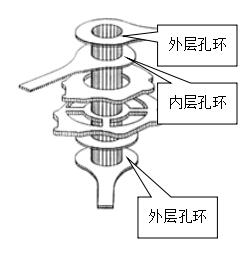
| Graphic circuit | Minimum line width / clearance of film | Minimum hole ring (calculation of inner layer of multilayer plate) |
Limit 0.075mm (single and double sided board) Routine 0.1mm Safety value 0.12mm |
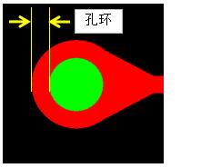
|
||||||||||||||||||||||||||||||||
| Single side 0.15mm (3 and 4 layers), safety value 0.2mm | ||||||||||||||||||||||||||||||||||||
| Single side 0.25mm (5 and 6-layer plates), safety value 0.3mm | ||||||||||||||||||||||||||||||||||||
| Single side 0.35mm (more than 6 layers) | ||||||||||||||||||||||||||||||||||||
| Minimum hole ring (outer layer of multilayer plate) | Single side 0.1mm, safety value 0.15mm | |||||||||||||||||||||||||||||||||||
| Process | Item | Internal capacity | Routine regulation | Graphical representation | ||||||||||||||||||||||||||||||||
| Graphic circuit | Minimum line width / clearance of film | Npth hole to line distance minimum | 0.1mm,Safety value 0.2mm (drilling) |
|
||||||||||||||||||||||||||||||||
| 0.15mm,Safety value 0.25mm (steel die punching) | ||||||||||||||||||||||||||||||||||||
| Minimum line width / clearance of 1 / 3 oz bottom copper | 0.05/0.04mm(Line compensated) | |||||||||||||||||||||||||||||||||||
| Minimum line width / clearance of 1 / 2 oz bottom copper | 0.06/0.07mm(Line compensated) | |||||||||||||||||||||||||||||||||||
| Minimum line width / clearance of 1oz bottom copper | Single panel:0.07/0.08mm(Line compensated) | |||||||||||||||||||||||||||||||||||
| Double sided board:0.08/0.09mm(Line compensated) | ||||||||||||||||||||||||||||||||||||
| Minimum line width and line distance of outer layer of hard and soft binding plate | 0.11/0.09mm(Line compensated) | |||||||||||||||||||||||||||||||||||
| Minimum line width / clearance of multilayer soft board | 0.09/0.07mm(Line compensated) | |||||||||||||||||||||||||||||||||||
| Etching compensation (overall): 1 oz copper | 0.03-0.04mm | |||||||||||||||||||||||||||||||||||
| Etching compensation (overall): 1 / 2 oz copper | 0.02-0.03mm | |||||||||||||||||||||||||||||||||||
| Etching compensation (overall): 1 / 3 oz copper | 0.015-0.02mm | |||||||||||||||||||||||||||||||||||
| Note: all independent lines shall be increased by 0.01-0.02MM (overall) on the basis of overall compensation; the minimum distance between lines shall be 0.04mm. | ||||||||||||||||||||||||||||||||||||
| Dry film | Counterpart tolerance | ±0.05mm |
|
|||||||||||||||||||||||||||||||||
| Deviation of figures on both sides (degree of coincidence) | ±0.05mm | |||||||||||||||||||||||||||||||||||
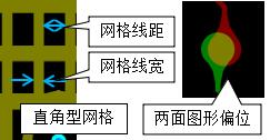
| Minimum grid (area) | 0.2 × 0.2mm (45 ° angle is the best) | |||||||||||||||||||||||||||||||||||
| Minimum grid line width / line spacing | 0.15/0.15mm | |||||||||||||||||||||||||||||||||||
| Solder resist | Solder resist | Minimum single side of opening distance from pad | 0.05mm,Safety value 0.075mm |
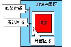
|
||||||||||||||||||||||||||||||||
| Minimum width of green oil Bridge | 0.1mm | |||||||||||||||||||||||||||||||||||
| One side of green oil bridge cover line is large | 0.05mm, safety value 0.075mm | |||||||||||||||||||||||||||||||||||
| Green minimum window | Ø0.025mm,Safety value Ø 0.04mm | |||||||||||||||||||||||||||||||||||
| Ink thickness |
≥ 10um (9-25um in general), Crown product thermosetting oil: 9 -- 15um) |
|||||||||||||||||||||||||||||||||||
| Minimum negative word height / minimum line width of green oil | 1.0/0.15mm | |||||||||||||||||||||||||||||||||||
| Character | Character | Positive text minimum line width | 0.1mm,Safety value 0.13MM |
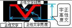
|
||||||||||||||||||||||||||||||||
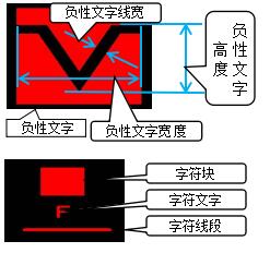
| Negative text minimum line width | 0.125mm,Safety value 0.15mm | |||||||||||||||||||||||||||||||||||
| Minimum height of text | 0.8mm | |||||||||||||||||||||||||||||||||||
| Minimum width of text | 0.8mm | |||||||||||||||||||||||||||||||||||
| Process | Item | Internal capacity | Routine regulation | Graphical representation | ||||||||||||||||||||||||||||||||
| Character | Minimum distance from character to pad | 0.15mm,Safety value 0.25mm |
|
|||||||||||||||||||||||||||||||||
| Minimum line width of character segment (non text) | 0.1mm,Best value 0.2mm | |||||||||||||||||||||||||||||||||||
| Minimum distance between character block and one side of pad | ≥0.2mm | |||||||||||||||||||||||||||||||||||
| Minimum distance from character to profile | 0.25mm | |||||||||||||||||||||||||||||||||||
| Carbon oil | Minimum carbon oil width / carbon oil spacing | 0.25/0.3mm | ||||||||||||||||||||||||||||||||||
| Minimum distance from profile edge | 0.3mm | |||||||||||||||||||||||||||||||||||
| Carbon oil resistance tolerance (3000 Ω high resistance) | ±400Ω | |||||||||||||||||||||||||||||||||||
|
ACP Conductive adhesive |
ACP thickness range | 15-25um | ||||||||||||||||||||||||||||||||||
| Number of conductive particles | >30个/mm² | |||||||||||||||||||||||||||||||||||
| Punching | Punching | Drilling accuracy tolerance | ±1mil(0.025mm) | |||||||||||||||||||||||||||||||||
| Fit | Coating film processing | Minimum drilling of covered membrane window |
Ø 0.4mm (drilling processing), Safety value 0.7mm |
|
||||||||||||||||||||||||||||||||
| Minimum square window with covering film | 0.6×0.6mm(Steel mold processing) | |||||||||||||||||||||||||||||||||||
| 0.5×0.5mm(Finishing die processing) | ||||||||||||||||||||||||||||||||||||
| Minimum opening space of covering film | 0.5mm(Precision die)、0.2mm(Laser engraving) | |||||||||||||||||||||||||||||||||||
| 0.15mm(Ordinary drilling) | ||||||||||||||||||||||||||||||||||||
| 0.2mm(Slotted hole, cross cov drilling Bridge) | ||||||||||||||||||||||||||||||||||||
| Minimum hole diameter of cutting cover film | 0.7mm | |||||||||||||||||||||||||||||||||||
| Cutting the minimum hole diameter of thermosetting adhesive and double-sided adhesive | 1.0mm | |||||||||||||||||||||||||||||||||||
| Minimum opening space of cover film cut by cutter | 0.15mm | |||||||||||||||||||||||||||||||||||
| Minimum opening of cover film for cutting machine | 0.6*0.6mm | |||||||||||||||||||||||||||||||||||
| Minimum punching of covering film | 0.6mm(Steel mold processing) | |||||||||||||||||||||||||||||||||||
| Double sided tape window is larger than FPC single side | 0.3-0.5mm | |||||||||||||||||||||||||||||||||||
| Distance from the edge of the cover film window to the edge of the pad or line | Products below 250 × 230mm: 0.05mm (safety value: 0.1mm) < products above 250 × 230mm: 0.075mm (safety value: 0.15mm) | |||||||||||||||||||||||||||||||||||
| Alignment tolerance of covering film and auxiliary materials | ± 0.15mm, safety value ± 0.2mm | |||||||||||||||||||||||||||||||||||
| Overflow of covering film (single side) |
Regular 0.08-0.12mm Limit 0.03mm (TPX pressing) |
|||||||||||||||||||||||||||||||||||
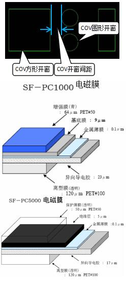
| Electromagnetic membrane | SF-PC5000/5500/5900 Black electromagnetic film minus release film thickness | 22um/22um/9um | ||||||||||||||||||||||||||||||||||
| Process | Item | Internal capacity | Routine regulation | Graphical representation | ||||||||||||||||||||||||||||||||
| Fit | Electromagnetic membrane | Sf-pc1000 silver electromagnetic film minus release film thickness | 32.1um |
|
||||||||||||||||||||||||||||||||
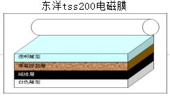
| Tss200 / tss100 black electromagnetic film | 22um/12um | |||||||||||||||||||||||||||||||||||
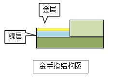
| Electroplate | Surface treatment | Nickel plating thickness (plating) | 2.54-9um(Normal value 2-6um) |
|
||||||||||||||||||||||||||||||||
| Thickness of gold plating (plating) |
0.025-0.2um (Normal value 0.025-0.075um) |
|||||||||||||||||||||||||||||||||||
| Nickel thickness | 1-6um (conventional 1-3um or 2-5um) | |||||||||||||||||||||||||||||||||||
| Thickness of gold deposit |
0.025-0.125um (routine value 0.025-0.075um) |
|||||||||||||||||||||||||||||||||||
| Tin plating thickness | 3-10um | |||||||||||||||||||||||||||||||||||
| Thickness of tin deposit | 0.6-1.2um | |||||||||||||||||||||||||||||||||||
| OSP Thickness | 0.3-0.5um | |||||||||||||||||||||||||||||||||||
| If the customer has special requirements, control according to the customer's requirements | ||||||||||||||||||||||||||||||||||||
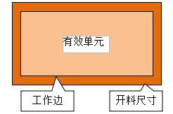
| Punching shear | Profile punching | Outline Tolerance |
± 0.05mm (high precision die) ± 0.07mm (precision mold, etching knife mold) ± 0.1mm (ordinary steel mold, simple steel mold) ± 0.2mm (common cutter die) |
|
||||||||||||||||||||||||||||||||
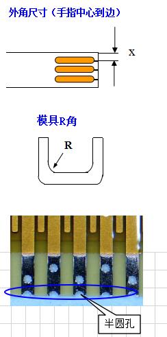
| Tolerance of external angle dimension (finger center to edge) | ± 0.05mm (high precision die)± 0.07mm (precision die making)± | |||||||||||||||||||||||||||||||||||
| ± 0.1mm (ordinary steel mold making, etching knife mold) | ||||||||||||||||||||||||||||||||||||
| Transition fillet allowed for sharp corner of profile | R≥0.20mm | |||||||||||||||||||||||||||||||||||
| The minimum distance from the center of the positioning hole to the profile edge | 2mm | |||||||||||||||||||||||||||||||||||
| Minimum distance between units | ≥ 0.5mm (suitable for jumping, generally 1-2mm) | |||||||||||||||||||||||||||||||||||
| Distance between profile edge and shear line | ≥ 2.0mm (cutter die), ≥ 2.5mm (manual) | |||||||||||||||||||||||||||||||||||
| Center distance of positioning hole (Ø 2.0mm) from shear line | ≥ 2.5mm (cutter die), ≥ 3mm (manual) | |||||||||||||||||||||||||||||||||||
| Minimum diameter of semicircle hole | 0.25mm, safety value 0.3mm | |||||||||||||||||||||||||||||||||||
| Minimum distance from line to board edge | 0.40mm (hand cut) | |||||||||||||||||||||||||||||||||||
| 0.3mm (common cutter die) | ||||||||||||||||||||||||||||||||||||
| 0.15mm (steel mold, etching knife mold) | ||||||||||||||||||||||||||||||||||||
| 0.1mm (precision die) | ||||||||||||||||||||||||||||||||||||
| Process | Item | Internal capacity | Internal capacity | Graphical representation | ||||||||||||||||||||||||||||||||
| Punching shear | Profile punching | The minimum distance between the line and the board edge is 500mm, and the product is arranged without gaps. | 0.3mm(Cutter die) | |||||||||||||||||||||||||||||||||
|
V-cut Milling plate V-CUT |
Hard and soft joint plate | Diameter of Gong knife | Min. δ 0.8mm (min. inner arc radius r0.4mm) |
|
||||||||||||||||||||||||||||||||
| Tube hole | NPTH孔 Ø1.0mm | |||||||||||||||||||||||||||||||||||
| Tolerance | Milling plate peripheral tolerance±0.13mm | |||||||||||||||||||||||||||||||||||
| Minimum distance from line to board edge | 0.2mm(Edge of Gong) | |||||||||||||||||||||||||||||||||||
| FR4 with the thinnest total thickness of V-CUT | 0.3mm | |||||||||||||||||||||||||||||||||||
| Shallowest depth of V-CUT | 0.08mm(Bevel angle:45°) | |||||||||||||||||||||||||||||||||||
| Test | Flying needle test | Minimum line width / distance of flying pin test | 0.05/0.05mm | |||||||||||||||||||||||||||||||||
| Maximum height drop of test point | 1.5mm | |||||||||||||||||||||||||||||||||||
| Finished product thickness | Finished product thickness | Thickness tolerance of finished product (0.05-0.10 mm) | ±0.015mm |
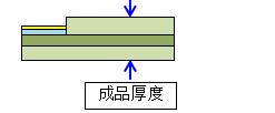
|
||||||||||||||||||||||||||||||||
| Thickness tolerance of finished product(0.11-0.2mm) | ±0.02mm | |||||||||||||||||||||||||||||||||||
| Thickness tolerance of finished product(0.21-0.40mm) | ±0.03mm | |||||||||||||||||||||||||||||||||||
| Multilayer hard and soft combination board | Determined according to specific plate arrangement structure | |||||||||||||||||||||||||||||||||||
| Impedance | Impedance tolerance | Single point impedance tolerance | ﹢/-10% | |||||||||||||||||||||||||||||||||
| Differential impedance tolerance | ﹢/-10% | |||||||||||||||||||||||||||||||||||
| Board type | Double sided board(100+/-10欧) |
1MIL 1/3OZ Non adhesive material 1.5MIL 1/3OZ Non adhesive material 1/2MIL 1/3OZ Gum material |
||||||||||||||||||||||||||||||||||
| Multilayer board | Match according to actual materials | |||||||||||||||||||||||||||||||||||
| SMT | SMT | Antistatic grade | Class A |
|
||||||||||||||||||||||||||||||||
| Dustless grade | Level 100 thousand | |||||||||||||||||||||||||||||||||||
| Minimum components | Routine 0201, limit 01005 | |||||||||||||||||||||||||||||||||||
| Minimum component spacing | Routine 0.3mm, limit 0.2mm | |||||||||||||||||||||||||||||||||||
| Min IC pitch | 0.3mm | |||||||||||||||||||||||||||||||||||
| Min connector pitch | 0.3mm | |||||||||||||||||||||||||||||||||||
| Min BGA pitch | 0.3mm | |||||||||||||||||||||||||||||||||||
| Maximum mosaic size | Conventional 250 * 240mm limit 330 * 240mm | |||||||||||||||||||||||||||||||||||
| Maximum board step | Normal ≤ 0.3mm limit ≤ 0.35mm | |||||||||||||||||||||||||||||||||||
| Type of solder paste | Lead free halogen free | |||||||||||||||||||||||||||||||||||
| Solder paste printing thickness | 120-180um | |||||||||||||||||||||||||||||||||||
| Process | Item | Internal capacity | Routine regulation | Graphical representation |
| SMT | SMT | Minimum tin area | 0.3*0.25mm |
|
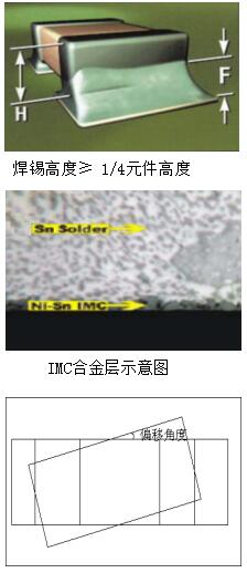
| Solder height | Element height more than 1 / 4 | |||
| Tin height on element pin | Greater than 1 / 2 of element pin | |||
| IMC alloy layer thickness | 1-3um | |||
| Number of temperature zone of hot air reflow welding | 10 temperature zone | |||
| Reflow temperature | Maximum 250 degrees centigrade | |||
| Manual welding temperature | 280-320℃ | |||
| Deviation tolerance of SMD | ±50um | |||
| Connector alignment tolerance | ±50um | |||
| IC alignment tolerance | ±50um | |||
| Led alignment tolerance | ±50um | |||
| Led offset angle | 1° | |||
| Led parallelism tolerance | ±50um | |||
| AOI inspection capability |
General: chip minimum: 0201, IC spacing: pitch=0.3mm; Limit: chip Min: 01005, IC spacing: pitch=0.3mm |
|||
| ICT test | 1200 points | |||
| Glue | UV adhesive, thermosetting adhesive, underfill (bottom filling) | |||
| Dispensing overflow tolerance (dispensing side) | ±50um | |||
| Dispensing overflow tolerance (non dispensing side) |
±50um |
Online
Service
ConsultationTime:9:00-18:00
Hot
Line
0755-29961800
7*24H Service
Follow
Wechat
 Website